Electronics Manufacturing Services


Electronics Manufacturing Services (EMS)
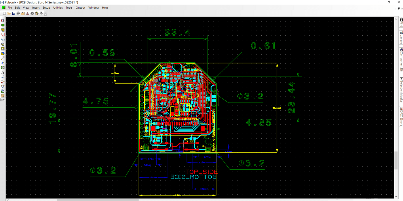
bpro has PCB design service activity which is carried out by a team of highly experienced professionals dedicated to customer services and interaction. We also undertake customized PCB design for various Form factors with very high mechanical constraints.

Services
PCB Design
Optimizing PCB layout design for manufacturability is one of the most crucial aspects of any product’s development process. Key decisions made during the design stage often have a tremendous impact on the cost and success of your product’s manufacturing and production.
Layers
Professional PCB Design Services of all types, including, Single-Layer, Double-Layer and Multi-Layer up to 12 Layers.
Layouts
Highly Complex & Dense PCB layout designs done with speed & accuracy
Services
Advanced component footprints & library creation including BGA, QFN packages as per IPC standards
Reverse Engineering
Reverse engineering services to correct flaws or to optimize existing PCB designs
Upgrade
Upgrade old PCB’s with outdated & obsolete components to the latest technology with widely available SMT components
Testing
Electrical & Functional Testing services of the designed PCB
We have experience with various PCB CAD tools with our primary tool being PULSONIX.


ELECTRONICS ASSEMBLY & MANUFACTURING
PCB Prototyping
PCB Testing
Wave Soldering
SMT Soldering
Manufacturing Machine We Use
SMT S10 YAMAHA PICK AND PLACE MACHINE
Board size : (with buffer unused) Min. L 50 x W 30 mm to
Max. L 1,330 x W 510 mm
Board thickness: 0.4 – 4.8 mm
Placement speed : (12 heads + 2 theta)
Opt. Cond. : 0.08 sec/CHIP (45,000CPH)
Placement accuracy A (μ+3 ) : CHIP +/- 0.040 mm, IC +/- 0.025 mm
Placement angle: +/-180 degrees
Component height: Max. 30 mm *1
KONARK 145 RE FLOW OVEN
Maximum PCB Width : 300 mm
Heating Length : 1550 mm
Max Temperature : 300˚C
Maximum Conveyor Speed : 2 m/min / 200 CPM
Clearance above Mesh : 60 mm
EMST PLCTT Wave Soldering
Overall dimensions : L – 1730 mm, W – 880 mm, H – 825 mm
Weight : 200 kg. (441 lb) max weight, without solder alloy
Supply voltage : Standard – 415 V, 3 phase, 50 Hz
Power consumption : 5 kVA total max
SEMI AUTO SCREEN PRINTER
Pcb size : 400 mm x 250 mm
Printing table size : 500 mm x 300 mm
Stencil size : adj. Up to 22” x 22”
Squeeze speed : 0-100 mm/sec
Power : 220v/ 50hz,
Pneumatic : 3cfm @ 5-7kg/cm 2

